2-D semiconductor contact resistances approach the quantum limit
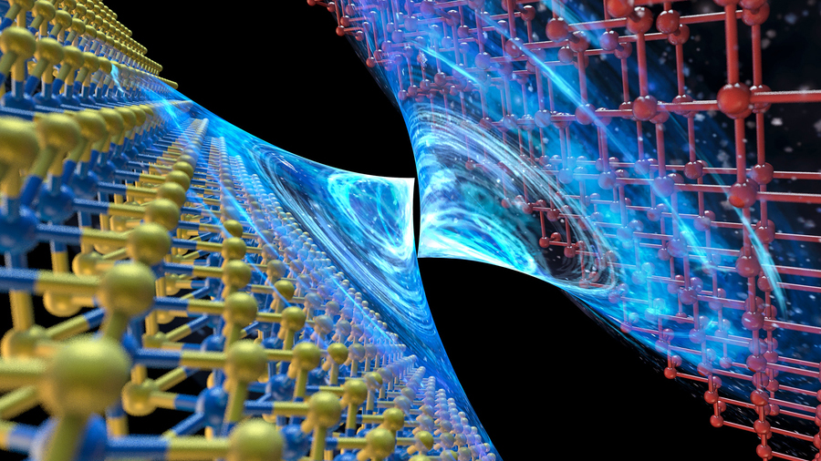
A paper co-authored by Berkeley EECS Prof. Jeffrey Bokor, his postdoc Yuxuan Lin, Berkeley Physics Prof. Alex Zettl, his postdoc Cong Su, and researchers at MIT, among others, describes a more efficient method of connecting atomically thin 2-D materials to other chip elements, making them a more promising alternative to 3-D silicon-based transistors. The paper, which was published in Nature, is titled “Ultralow contact resistance between semimetal and monolayer semiconductors.” It describes how using the element bismuth (in the place of ordinary metals) for connections in monolayer materials can create contact resistances that approach the quantum limit and make it possible to develop smaller devices. “We resolved one of the biggest problems in miniaturizing semiconductor devices, the contact resistance between a metal electrode and a monolayer semiconductor material,” says Su. “Through this approach,” the paper states, “we achieve zero Schottky barrier height, a contact resistance of 123 ohm micrometres and an on-state current density of 1,135 microamps per micrometre on monolayer MoS2; these two values are, to the best of our knowledge, the lowest and highest yet recorded, respectively.”